
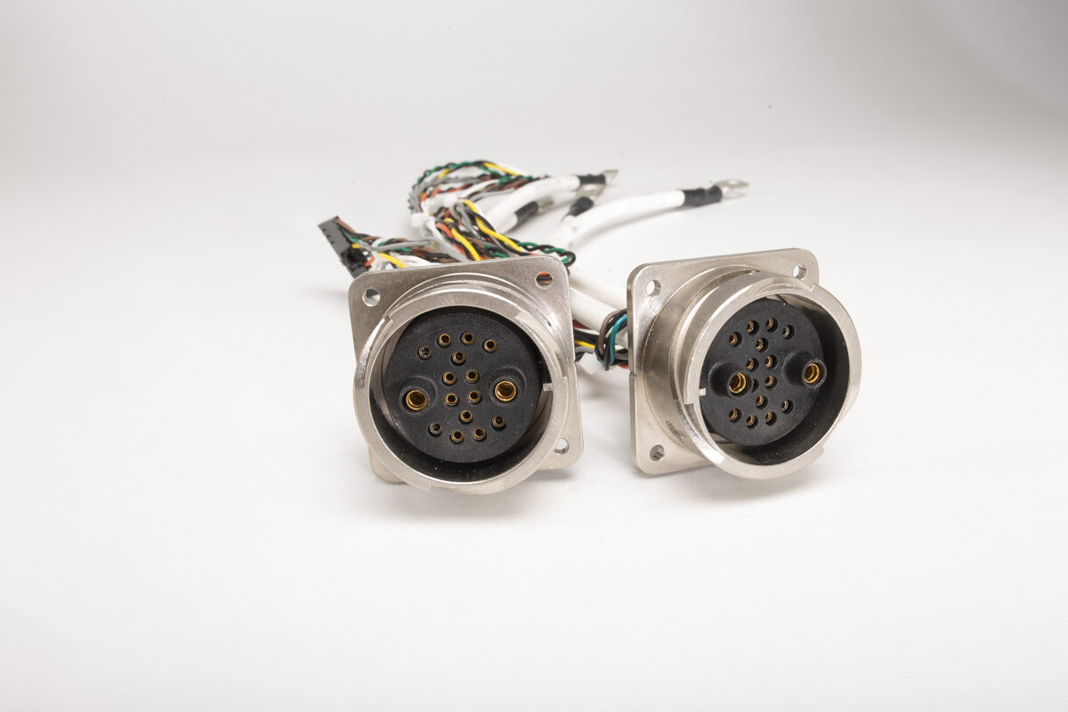
The termination region — where the cable transitions into the connector — concentrates more sources of electrical risk in less space than almost any other location in a high-voltage assembly. Many partial-discharge and dielectric failures originate here when field stress, material interfaces, trapped air, or mechanical strain are not explicitly controlled. The mechanisms are understood, and with the right engineering approach they are preventable.
Termination Engineering · 10 kV – 250 kV DC · Aerospace · Defense · Medical · Scientific
What "Termination" Actually Means — and What It Doesn't
In connector and cable assembly practice, the term termination is used loosely to mean almost any junction — a contact crimp, a solder joint, even a connector mating interface. That usage creates confusion when discussing high-voltage failure modes, so it is worth being precise.
For the purposes of this note, termination design refers to the engineered transition zone between the cable insulation system and the connector body insulation — the region where the cable's dielectric structure ends and the connector's dielectric structure begins, including the conductor transition, shield cutback (if applicable), void elimination strategy, and strain relief geometry.
In power-cable termination practice, the termination must generally address four functions: provide electric stress control at the point of shield cutback, provide external leakage insulation appropriate to the environment, seal the cable end against the external environment, and mechanically support the conductor at the point of transition. IEEE Std 48-2020, which addresses AC terminations for shielded cables with laminated insulation rated 2.5 kV through 765 kV and extruded insulation rated 2.5 kV through 500 kV, provides test procedures and requirements in this context. Each of these four functions has a corresponding failure mode in practice.
Note on DC vs. AC Field Distribution
IEEE Std 48 and IEC 60840 address AC cable systems. For DC applications, the steady-state electric field distribution is governed primarily by the conductivity/resistivity of the dielectric materials rather than permittivity alone — which means that at elevated temperature, resistive grading can shift field distribution in ways that capacitive or geometric grading alone may not fully control. DC-rated connector assemblies above 10 kV require explicit analysis of the resistive field distribution across the operating temperature range. This is one reason that DC high-voltage design cannot be directly adapted from AC cable accessory practice.
Where Termination Failures Start
Many high-voltage dielectric failures in termination regions share a common initiating mechanism: partial discharge (PD) in a void, gap, contamination path, or field concentration point within or adjacent to the insulation system at the termination region. The specific physical location varies by design and fabrication method, but the four most consequential origination sites are:
- The shield cutback edge. In shielded assemblies, the abrupt end of the conductive shield disrupts the coaxial field geometry, concentrating field lines at the edge. Research cited in the technical literature on shielded cable accessories confirms that ungraded shield cutback edges operate at field intensities far above the design stress of the surrounding insulation — in some cases several times the bulk insulation stress — making this the highest-risk single location in a shielded termination.
- Material interface boundaries. The junction between cable insulation and connector body insulation (or potting compound) is a material discontinuity. If the two materials have different relative permittivities, the field distribution across the boundary is non-uniform. Any gap — even a few microns wide — at this interface becomes a site where the local field far exceeds the breakdown strength of air.
- Fabrication voids in potted terminations. Conventional atmospheric potting traps air during cure. In complex termination geometries, blind cavities and undercuts can retain bubbles that survive mixing and pouring. These voids are frequently invisible in the finished assembly. At elevated voltage they become PD sites.
- Mechanical deformation under load. In service, terminations experience tension, bending, vibration, and thermal cycling. A termination that passes electrical testing at ambient after fabrication may develop gaps or delaminations at cryogenic temperatures or after mechanical fatigue. This failure mode is particularly relevant to aerospace and defense applications where qualification testing must account for the full environmental envelope.
Why Standard Assembly Practice Falls Short
Atmospheric potting is difficult to validate as void-free
The most common method for insulating multi-conductor high-voltage terminations is to fill the backshell or termination cavity with a castable compound — silicone RTV, polyurethane, or epoxy — applied at atmospheric pressure. The difficulty is that complex termination geometries contain blind cavities, conductor bundles, and abrupt cross-section changes that trap air as the compound flows in. The compound cures around the trapped bubbles. Routine production inspection may not reliably detect these voids: visual inspection sees only the surface, and conventional X-ray may detect larger voids but can miss small voids, thin gaps, or interface defects depending on material contrast, geometry, and resolution.
At lower voltages, small air voids may not produce damaging partial discharge. As voltage increases into the high-voltage range — especially in compact connector geometries — air-filled voids in the termination region become a predictable PD risk unless the geometry, materials, pressure environment, and test margins are explicitly controlled. The dielectric strength of air at sea level is approximately 3 kV/mm; silicone rubber is 18–25 kV/mm depending on compound and geometry. A void concentrates the local field to well above the surrounding material's design stress. Partial discharge initiates in the void, erodes the adjacent solid insulation over time, and progresses to dielectric breakdown.
Standard inspection cannot detect the failure before it occurs
Hi-pot testing — applying a fixed DC or AC withstand voltage for a defined period — is a go/no-go screen. It confirms that the assembly does not fail at the test voltage at the moment of test. It does not detect incipient voids, marginal insulation, or latent PD that initiates below the test voltage threshold. For example, depending on geometry and void location, an assembly that passes a 50 kV hi-pot screen could still exhibit PD at a 30 kV operating voltage if small voids or interfacial gaps are present.
The technically correct screen for void-related failure is corona / partial discharge testing — measuring the voltage at which discharge activity initiates (the partial discharge inception voltage, or PDIV) and confirming that this threshold exceeds the rated operating voltage by an appropriate margin. This test requires instrumentation, fixturing, shielding, and environmental controls that are not part of ordinary low-voltage cable assembly production.
Common Misconception
Passing a hi-pot test does not confirm the absence of partial discharge at operating voltage. Hi-pot and partial discharge inception testing are complementary screens — they detect different failure conditions. An assembly can pass hi-pot and still exhibit PD at rated voltage if the PDIV is between the operating voltage and the hi-pot test voltage.
Altitude degrades air-gap breakdown voltage significantly
The dielectric strength of air is pressure-dependent. At sea level, air breaks down at approximately 3 kV/mm under uniform-field conditions. At 70,000 feet, ambient pressure is only a few percent of sea-level pressure — approximately 4–5% under a standard-atmosphere model — and the Paschen curve shows that breakdown voltage drops significantly at reduced pressure, reaching a minimum (the Paschen minimum) before rising again at very low pressures. For aircraft and aerospace systems operating at altitude or in depressurized enclosures, any air void that is electrically benign at sea level may become a PD site at altitude.
This is why the design target for aerospace high-voltage cable assemblies is to avoid air-filled voids in electrically stressed regions, minimize trapped gas in the dielectric path, and verify adequate PDIV margin under the relevant pressure environment — not simply to ensure that any voids present are small enough to be tolerable at ground level.
Build-to-print assembly does not address field grading
Most cable assembly procurement specifications define the cable, the connector, the termination length, and the electrical performance requirements — and leave the termination design to the manufacturer's discretion. A manufacturer without high-voltage engineering capability will apply a standard potting process, perform a hi-pot screen, and deliver an assembly that may or may not have the necessary field grading geometry at the shield cutback edge.
Field grading at the shield cutback — the controlled redistribution of field lines away from the abrupt shield edge — is not a feature that emerges automatically from assembly practice. It requires explicit engineering: geometric shaping of the insulation profile, selection of materials with defined permittivity relationships, or the application of stress-grading materials. These decisions must be made at the design stage, not the assembly stage.
How Geometry and Physics Determine the Outcome
The governing physics of the termination region is the same as elsewhere in a high-voltage system: the electric field concentrates at geometric discontinuities, at material boundaries where permittivity changes, and at any location where the conductor-to-ground distance decreases abruptly. What makes the termination region different is the density of these features in a small space.
In the cable body, the field distribution is well-defined: a coaxial geometry with radially symmetric field, calculable from first principles, with no material discontinuities in the dielectric path. In the termination region, the coaxial geometry ends, the conductor transitions in cross-section, the shield terminates, the cable insulation gives way to connector body insulation, and the geometry becomes three-dimensional and irregular. Each of these changes affects the field distribution, and their interactions are not amenable to simple analytical approximation.
This is the reason Caton performs electrostatic field modeling — using finite-element simulation tools — before any termination design goes to tooling. Field modeling makes the distribution visible, identifies concentration points, and allows evaluation of design changes before hardware is built. A termination design that looks adequate from dimensional inspection may still exhibit unacceptable field concentration at a specific geometric feature — and that feature will not become visible until either the simulation or a failure reveals it.
Engineering Note — Field Modeling
Caton uses Electro V10.2 for electrostatic field analysis of termination geometry prior to tooling. The analysis confirms that field intensity at all material interfaces and geometric transitions remains within the design margins for the insulation system selected. This step occurs before any prototype hardware is built — because fabrication and test are not cost-effective substitutes for geometry analysis.
How Caton Addresses It — Engineering Controls for High-Voltage Termination Integrity
- Electrostatic field modeling before tooling. Caton models the termination geometry in Electro V10.2 before any design is committed to tooling. The simulation identifies field concentration points at shield cutback edges, material interfaces, and conductor transitions, and confirms that the field intensity at all locations falls within the design margins of the selected insulation system. Designs that fail this analysis are modified before hardware is built.
- In-house overmolding — the interface is molded, not assembled. For single-conductor terminations, Caton forms the termination insulation by injection molding rather than potting. Tooling controls the termination geometry precisely; the mold fills under pressure before cure, substantially reducing void risk compared with atmospheric potting and improving control of the dielectric path. The result is a molded, bonded transition from cable insulation through connector body — rather than a manually assembled or post-filled interface — which reduces the likelihood of interfacial gaps or delamination when the material system and surface preparation are properly controlled.
- Vacuum-applied potting for multi-conductor terminations. Where potting is required — as in multi-conductor backshell configurations — Caton applies the compound under vacuum, evacuating the termination cavity before introduction of the potting material. When the vacuum is released, atmospheric pressure drives the compound into all cavities and against all surfaces. This approach directly addresses void formation in complex geometries that cannot be reliably filled by atmospheric potting methods.
- 100% corona / partial discharge testing on applicable high-voltage assemblies — no sampling. Every applicable high-voltage production assembly undergoes corona testing in one of Caton's four corona test cages. Testing verifies the partial discharge inception voltage (PDIV) of the complete assembly — cable, terminations, and connector interface — against an acceptance criterion established relative to the rated operating voltage and required design margin. This is a 100% production screen for applicable assemblies, not a periodic sample. Hi-pot testing is performed on every assembly as a separate screen for dielectric withstand integrity.
- Altitude qualification testing for aerospace and airborne applications. For assemblies intended for airborne or altitude-sensitive applications, Caton performs simulated altitude testing in an in-house Tenny altitude chamber. Testing confirms electrical performance at the ambient pressure corresponding to the application's operational envelope — because void-related partial discharge that is inactive at ground-level pressure may initiate at altitude.
- Termination geometry designed for mechanical stability through the full service environment. Caton's termination designs account for the differential thermal expansion between cable insulation, conductor, and connector body, and include sufficient strain relief geometry to prevent bending loads from introducing movement at the insulation interface. Designs intended for thermal cycling environments are analyzed for interface stability across the operating temperature range before qualification.
What to Ask Your Current or Prospective Supplier
The following questions separate suppliers with genuine high-voltage engineering capability from those applying standard cable assembly practice to a high-voltage application. A supplier that cannot answer these questions with specific design rationale, process controls, and test evidence may be treating a high-voltage termination as a conventional cable assembly problem.
- Do you perform electrostatic field analysis of the termination geometry before committing a design to tooling? What software do you use, and can you show us the field plots for this termination?
- How do you eliminate voids in the termination region? Specifically, do you use vacuum potting, in-house overmolding, or atmospheric-applied potting? What controls verify void-free fill in the finished assembly?
- Do you perform partial discharge (corona) testing on production assemblies — 100% of units, or a sample? What is your PDIV acceptance threshold relative to the rated operating voltage?
- Have you tested this termination design at the ambient pressure corresponding to our application altitude? Do you have in-house altitude test capability, or do you subcontract this testing?
- How does your termination design address field concentration at the shield cutback edge? Is the stress control approach geometric, material-based, or a combination — and what analysis supports the design?
- Has this termination design been thermally cycled through the full operating temperature range followed by electrical test? What does the qualification data show about PDIV stability after thermal cycling?
Technical References
- IEEE Std 48-2020. IEEE Standard for Test Procedures and Requirements for Alternating-Current Cable Terminations Used on Shielded Cables Having Laminated Insulation Rated 2.5 kV through 765 kV or Extruded Insulation Rated 2.5 kV through 500 kV. IEEE, 2020. Establishes test procedures and requirements for AC shielded-cable terminations in power-cable practice — the context in which terminations must address electric stress control, external leakage insulation, environmental sealing, and mechanical support. Referenced in the definitions section of this note.
- IEC 60840:2020. Power cables with extruded insulation and their accessories for rated voltages above 30 kV (Um = 36 kV) up to 150 kV (Um = 170 kV) — Test methods and requirements. IEC, 2020. IEC 60840 is not a connector-specific standard, but it provides useful context for how high-voltage cable-system standards treat partial discharge testing and accessory qualification. The PD acceptance criterion — no detectable discharge exceeding 5 pC at 1.5 U₀ — illustrates what the standards consider adequate margin. Referenced in the testing section of this note.
- IEEE Std 400.3-2022. IEEE Guide for Partial Discharge Field Diagnostic Testing of Shielded Power Cable Systems. IEEE, 2022. Explains the distinction between PDIV (partial discharge inception voltage) and PDEV (extinction voltage), the significance of space charge accumulation, and why hi-pot testing and PD testing detect different failure conditions. Supports the discussion in the "Why Standard Assembly Practice Falls Short" section.
- Eoll, C.K. (1975). "Theory of stress distribution in insulation of high-voltage DC cables." IEEE Transactions on Electrical Insulation, EI-10(1), 27–35. Establishes the distinction between AC and DC field distribution in cable insulation — AC field governed by permittivity, DC field governed by resistivity. Directly relevant to the engineering note on DC field distribution in this application note.
- NASA-STD-8739.4A (with current changes). Workmanship Standard for Crimping, Interconnecting Cables, Harnesses, and Wiring. NASA, current revision. Provides an aerospace workmanship baseline for cable and harness assemblies; high-voltage specialty requirements should be added where the application requires corona control, dielectric stress management, or altitude performance. Referenced in context of mechanical design and strain relief discussion.
References are provided to support the technical claims in this application note and to allow engineers to verify source material independently. Where standards are cited, the edition current at time of publication applies. Contact our engineering team with questions about how any reference applies to a specific application.